advertisement

Freescale Semiconductor, Inc.
Order this document by
MC68EN302/D
MC68EN302
Product Brief
Integrated Multiprotocol Processor with Ethernet
Freescale introduces a version of the well-known MC68302 Integrated Multiprotocol Processor (IMP) with
Ethernet and DRAM controllers. It is known as the MC68EN302, and expands a family of devices based on the
MC68302.
The Ethernet controller has a 16-bit interface, resides on the 68000 bus and provides complete IEEE 802.3
compatibility. The programming model is adopted from the standard 68302 programming model. The DRAM controller is adopted from the MC68306 product. It is enhanced to support both parity and external bus masters.
The MC68EN302 is packed in a low profile 144 TQFP.
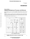
MC68EN302
MC68302
1 GENERAL-
PURPOSE
DMA
CHANNEL
3 TIMERS
AND
ADDITIONAL
FEATURES
68000
SYSTEM BUS
MC68000
INTERRUPT
CONTROLLER JTAG
IEEE 1149.1
MICROCODED
COMMUNICATIONS
CONTROLLER
(RISC)
6 DMA
CHANNELS
1152 BYTES
DUAL-PORT
RAM
PERIPHERAL
BUS
MODULE BUS
CONTROLLER
ETHERNET
CONTROLLER
DRAM
CONTROLLER
OTHER
SERIAL
CHANNELS
3 SERIAL
CHANNELS
Figure 1. MC68EN302 Block Diagram
This document contains information on a product under development. Freescale reserves the right to change or discontinue this product without notice.
SEMICONDUCTOR PRODUCT INFORMATION
1995
For More Information On This Product,
Go to: www.freescale.com
Freescale Semiconductor, Inc.
FEATURE LIST
The following features are incorporated into the MC68EN302 device:
• Full Complement of Existing Three SCC’s Plus Ethernet Channel
• Ethernet Channel Fully Compliant with IEEE 802.3 Specification.
• Supports Data Rates up to 10 Mbps.
• Supports the “68302” Style Programming Model.
• On-Chip Descriptors Lower Processor Bus Bandwidth Requirements.
• Separate 128 Byte FIFOs for Transmit and Receive.
• Automatic Internal Retransmission (which Frees the Processor Bus).
• Automatic Internal Flushing of Receive FIFO During Collisions (which Frees the Processor Bus).
• Dynamic Bus Sizing Support for 8-Bit Devices
• Glueless Dynamic RAM Controller without External Bus Master
• Address Muxing Support for External Bus Masters Using DRAM Controller
• Fully IEEE 1149.1 JTAG Compliant
• 144 TQFP Package for Up to 25 MHz
ETHERNET CONTROLLER
The Ethernet controller consists of a Ethernet protocol core, transmit and receive FIFOs, and a 16-bit wide data/control interface to a 68000 bus (refer to Figure 2). The Ethernet protocol core (EPC) provides compatibility with the IEEE 802.3 Ethernet standard. The transmit and receive FIFOs allow automatic handling of collisions and collision fragments by the EPC, and they also provide for bus latency that can be encountered by the DMA channels. Separate DMA channels are used for transmit and receive data paths. A dual-port RAM is used for the on-chip buffer descriptors. A buffer descriptor control (BDC) block updates the buffer descriptors. Control status registers are used for direct control of all of the blocks in the Ethernet controller.
ETHERNET FEATURES
• Does Not Affect Performance of Existing SCCs
• 802.3 MAC Layer Support
• Compatible with 68160 EEST (Twisted Pair/AUI)
• Two Dedicated Ethernet DMA channels, Transmit and Receive
• Full-Duplex (Switched) Ethernet Support
• Up to 10 Mb/s Operation (20 Mb/s Full-Duplex)
• 128-Byte FIFO on both Transmit and Receive
• No CPU or Bus Overhead Required on Rx or Tx Frame Collisions
• 64 entry CAM with Hash Option
• 128 internal Buffer Descriptors
• Performs Framing Functions
MC68EN302 PRODUCT INFORMATION
For More Information On This Product,
Go to: www.freescale.com
Freescale Semiconductor, Inc.
• Full Collision Support
• Receives Back-to-Back Frames
• Detection of Receive Frames That Are Too Long
• Multi-Buffer Data Structure
• Supports 48-Bit Addressing
• Heartbeat Indication
• Transmitter Network Management and Diagnostics
• Receiver Network Management and Diagnostics
• Loopback Mode for Testing
• Non-Aggressive Deferral Option
• Heartbeat Status and Interrupt Option
• Graceful Stop Command
MODULE BUS
CONTROL
STATUS
REGISTERS
DESCRIPTOR
DUAL-PORT
RAM
2 DMA
CHANNELS
SYSTEM
INTERFACE
BUFFER
DESCRIPTOR
CONTROL
TRANSMIT
STATUS
ETHERNET
PROTOCOL
TRANSMIT
FIFO
RECEIVE
FIFO
ETHERNET
PROTOCOL
CORE
ADDRESS
RECOGNITION
DUAL-PORT
RAM
EEST INTERFACE
Figure 2. Ethernet Controller Block Diagram
MC68EN302 PRODUCT INFORMATION
For More Information On This Product,
Go to: www.freescale.com
Freescale Semiconductor, Inc.
MODULE BUS CONTROLLER
The MC68EN302 module bus controller provides basic interface capabilities to the module bus as well as basic system responsibilities. The features of the module bus controller are:
• Interface Between Internal 68000 bus and the Module Bus.
• Provision for Dynamic Bus Sizing, Using the Chip Select Logic of the 68302 Core.
• Handling of Interrupts for the Ethernet Controller and DRAM Controller.
• Coordination of Bus Mastership from External Sources, the Module Bus, and the MC68EN302 Core.
MC68EN302
INTERNAL
302 BUS
F
F
B
U
E
R
S
INTERNAL
68000 BUS
MODULE
BUS
CONTROLLER
MODULE BUS
ETHERNET AND
DRAM CONTROLLER
Figure 3. BusStructure
D
S
P
A
EXTERNAL
68000 BUS
DRAM CONTROLLER
• Provides two CAS lines
• Provides two RAS lines (two banks supported)
• DRAM address multiplexing on standard address bus
• Programmable up to three wait states
• 100 nS DRAM for zero wait states at 20 MHz
• 80 nS DRAM for zero wait states at 25 MHz
• CAS before RAS refresh and refresh support during system reset
MC68EN302 PRODUCT INFORMATION
For More Information On This Product,
Go to: www.freescale.com
Freescale Semiconductor, Inc.
• Programmable refresh period and pre-charge period
• RAS lines are separate from the four chip selects
• Refresh hidden from bus accesses
• Write protect option
• Each bank programmable size from 128Kbytes to 8Mbytes
ADDRESS 23–ADDRESS 0
BLOCKHIT0
BLOCKHIT1
ADDRESS
MULTIPLEXING
DRAM ADDRESS
ADDRESS
DECODE
AS
UDS
LDS
R/W
RAS/CAS
GENERATION
AMUX
RAS1, RAS0
CAS1, CAS0
DRAM_RW
CLK RFRESH
TIMER
Figure 4. DRAM Controller
MC68EN302 APPLICATIONS
The MC68EN302 is intended for low-end bridge and router applications. It has the three SCCs from the
MC68302, plus an additional Ethernet interface giving it a total of four serial interfaces.
Since the MC68EN302 has both the three SCCs as well as an Ethernet interface, it would be an excellent choice in an ISDN to Ethernet router.
For remote access dial-in, the MC68EN302 could be used in a dial-up modem that would connect to an
Ethernet LAN.
• Low End Bridges
MC68EN302 PRODUCT INFORMATION
For More Information On This Product,
Go to: www.freescale.com
Freescale Semiconductor, Inc.
• Industrial Control
• Remote LAN Access Points for Remote Dial-In
• PCMCIA Ethernet + WAN Cards
• Communication System Control Boards
• Intelligent Peripheral Chip to an 020/030
MC68EN302 PRODUCT INFORMATION
For More Information On This Product,
Go to: www.freescale.com
Freescale Semiconductor, Inc.
MC68EN302 PIN DESCRIPTION
NMSI1 / ISDN I / F
RXD1 / L1RXD
TXD1 / L1TXD
RCLK1 / L1CLK
TCLK1 / L1SY0 / SDS1
CD1 / L1SY1
CTS1 / L1GR
RTS1 / L1RQ / GCIDCL
NMSI2 / PIO
RXD2 / PA0
TXD2 / PA1
RCLK2 / PA2
TCLK2 / PA3
CTS2 / PA4
RTS2 / PA5
CD2 / PA6
RXD3 / PA8
TXD3 / PA9
RCLK3 / PA10
TCLK3 / PA11
CTS3 / SPRXD
RTS3 / SPTXD
CD3 / SPCLK
NMSI3 / SCP / PIO
IDMA / PAIO
DREQ / PA13 / WEL
DACK / PA14 / WEH
DRAM / IACK / PBIO
CAS0 / IACK7 / PB0
CAS1 / IACK6 / PB1
DRAMRW / IACK1 / PB2
AMUX / BRG1
RAS0 / BRG2 / SDS2 / PA7
RAS1 / BRG3 / PA12
OE / DONE / PA15
A0 / TOUT1 / PB4
TIN1 / PB3
TIN2 / PB5
TOUT2 / PB6
WDOG / PB7
TIMER / PBIO
PBIO (INTERRUPT)
PB8
PB9
PB10
PB11
MC68EN302
144-LEAD
CLOCKS
EXTAL
XTAL
CLKO
ADDRESS BUS
A23–A1
DATA BUS
D15–D0
BUS CONTROL
AS
R/W
UDS
LDS / DS
DTACK
BUS ARBITRATON
BR
BG
BGACK
SYSTEM CONTROL
RESET
HALT
BERR
PARITY1 / BUSW
PARITY0 / DISCPU
PARITYE / THREES
INTERRUPT CONTROL
IPL0 / IRQ1
IPL1 / IRQ6
IPL2 / IRQ7
FC0
FC1
FC2
AVEC / IOUT0
CHIP SELECT
CS0 / IOUT2
CS3–CS1
TESTING
TMS
TDI
TDO
TCK
TRST
ETHERNET
RX
TX
RENA
CLSN
RCLK
TENA
TCLK GND(16)
VDD (10)
MC68EN302 PRODUCT INFORMATION
For More Information On This Product,
Go to: www.freescale.com
Freescale Semiconductor, Inc.
Package Type
Thin Quad Flat Pack
(PV Suffix)
Thin Quad Flat Pack
(PV Suffix)
Table 1. MC68EN302 Ordering Information
Operating
Voltage
5V
Frequency
(MHz)
20
Temperature
0
°
C to 70
°
C
5V 25 0
°
C to 70
°
C
Order Number
MC68EN302PV20
MC68EN302PV25
Table 2. Documentation
Document Title
MC68302 User's Manual
M68000 Family Programmer's Reference Manual
The 68K Source
Order Number
MC68302UM/AD
M68000PM/AD
BR729/D
The MC68EN302 Addendum
Contents
Detailed information for design
M68000 Family Instruction Set
Independent vendor listing supporting software and development tools
Describes the differences between the
MC68302 and the MC68EN302
SEMICONDUCTOR PRODUCT INFORMATION
For More Information On This Product,
Go to: www.freescale.com
advertisement
* Your assessment is very important for improving the workof artificial intelligence, which forms the content of this project
Related manuals
advertisement