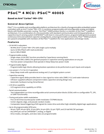
Block diagram. Infineon CY8C4045LQI-S412, CY8C4045LQI-S413, CY8C4025AZI-S413T, CY8C4024LQI-S412, CY8C4025AZQ-S403, CY8C4024LQI-S403T, CY8C4025LQI-S412, CY8C4025LQI-S402T, CY8C4045LQI-S411, CY8C4024AXI-S412
Add to My manuals58 Pages
advertisement

PSoC™ 4 MCU: PSoC™ 4000S
Based on Arm® Cortex®-M0+ CPU
Block diagram
Block diagram
PSoC™ 4000S
Architecture
32-bit
AHB-Lite
System Resources
Lite
Power
Sleep Control
WIC
POR
PWRSYS
REF
Clock
Clock Control
WDT
ILO IMO
Reset
Reset Control
XRES
Test
TestMode Entry
Digital DFT
Analog DFT
CPU Subsystem
SWD/TC
Cortex® M0+
48 MHz
FAST MUL
NVIC, IRQMUX
SPCIF
FLASH
32 KB
Read Accelerator
SRAM
4 KB
SRAM Controller
Peripherals
PCLK
System Interconnect (Single Layer AHB)
Peripheral Interconnect (MMIO)
ROM
8 KB
ROM Controller
Power Modes
Active/Sleep
DeepSleep
High Speed I/O Matrix & 2 x Programmable I/O
36x GPIOs, LCD
I/O Subsystem
PSoC™ 4000S devices include extensive support for programming, testing, debugging, and tracing both hardware and firmware.
The Arm® serial-wire debug (SWD) interface supports all programming and debug features of the device.
Complete debug-on-chip functionality enables full-device debugging in the final system using the standard production device. It does not require special interfaces, debugging pods, simulators, or emulators. Only the standard programming connections are required to fully support debug.
The PSoC™ Creator IDE provides fully integrated programming and debug support for the PSoC™ 4000S devices.
The SWD interface is fully compatible with industry-standard third-party tools. The PSoC™ 4000S provides a level of security not possible with multi-chip application solutions or with microcontrollers.
It has the following advantages:
• Allows disabling of debug features
• Robust flash protection
• Allows customer-proprietary functionality to be implemented in on-chip programmable blocks
Datasheet 7 002-00123 Rev. *O
2022-07-28
PSoC™ 4 MCU: PSoC™ 4000S
Based on Arm® Cortex®-M0+ CPU
Block diagram
The debug circuits are enabled by default and can be disabled in firmware. If they are not enabled, the only way to re-enable them is to erase the entire device, clear flash protection, and reprogram the device with new firmware that enables debugging. Thus firmware control of debugging cannot be over-ridden without erasing the firmware thus providing security.
Additionally, all device interfaces can be permanently disabled (device security) for applications concerned about phishing attacks due to a maliciously reprogrammed device or attempts to defeat security by starting and interrupting flash programming sequences. All programming, debug, and test interfaces are disabled when maximum device security is enabled. Therefore, PSoC™ 4000S, with device security enabled, may not be returned for failure analysis. This is a trade-off the PSoC™ 4000S allows the customer to make.
Datasheet 8 002-00123 Rev. *O
2022-07-28
advertisement
Related manuals
advertisement
Table of contents
- 1 General description
- 1 Features
- 3 Table of contents
- 4 1 Development ecosystem
- 4 1.1 PSoC™ 4 MCU resources
- 5 1.2 ModusToolbox™ software
- 6 1.3 PSoC™ Creator
- 7 Block diagram
- 9 2 Functional description
- 10 3 Functional definition
- 10 3.1 CPU and memory subsystem
- 10 3.2 System resources
- 12 3.3 Analog blocks
- 12 3.4 Programmable digital blocks
- 13 3.5 Fixed function digital
- 14 3.6 GPIO
- 14 3.7 Special function peripherals
- 15 4 Pinouts
- 17 4.1 Alternate pin functions
- 19 5 Power
- 19 5.1 Mode 1: 1.8 V to 5.5 V external supply
- 20 5.2 Mode 2: 1.8 V ± 5% external supply
- 21 6 Electrical specifications
- 21 6.1 Absolute maximum ratings
- 22 6.2 Device level specifications
- 27 6.3 Analog peripherals
- 32 6.4 Digital peripherals
- 36 6.5 Memory
- 37 6.6 System resources
- 41 7 Ordering information
- 43 8 Packaging
- 44 8.1 Package diagrams
- 49 9 Acronyms
- 53 10 Document conventions
- 53 10.1 Units of measure
- 54 Revision history